") 基于STM32H743I高性能400MHz 32位ARM MCU開發(fā)方案詳解
基于STM32H743I高性能400MHz 32位ARM MCU開發(fā)方案詳解

ST公司的STM32H743I是高性能工作頻率400MHz的32位ARM Cortex?-M7MCU,具有浮點單元(FPU),支持Arm?雙精度(IEEE 754兼容)和單精度數(shù)據(jù)處理指令和數(shù)據(jù)類型,集成了高達2MB閃存,1MB RAM,Art加速器,L1緩存,外設(shè)存儲器接口以及各種外設(shè),856 DMIPS/2.14 DMIPS/MHz (Dhrystone 2.1)。主要用在馬達驅(qū)動和應(yīng)用控制,醫(yī)療電子,工業(yè)應(yīng)用如PLC,逆變器和電路斷路器,打印機和掃描儀,告警系統(tǒng),視頻互連和HVAC,家庭音響,移動應(yīng)用和物聯(lián)網(wǎng),可穿戴如智能手表。本文介紹了STM32H743xI主要特性,框圖,以及評估板STM32H743I-EVAL主要特性,框圖,主要元件分布圖和電路圖,材料清單。
STM32H743xI devices are based on the high-performance Arm? Cortex?-M7 32-bit RISC core operating at up to 400 MHz. The Cortex? -M7 core features a floating point unit (FPU) which supports Arm? double-precision (IEEE 754 compliant) and single-precision data-processing instructions and data types. STM32H743xI devices support a full set of DSP instructions and a memory protection unit (MPU) to enhance application security.
STM32H743xI devices incorporate high-speed embedded memories with a dual-bank Flash memory up to 2 Mbytes, 1 Mbyte of RAM (including 192 Kbytes of TCM RAM, 864 Kbytes of user SRAM and 4 Kbytes of backup SRAM), as well as an extensive range of enhanced I/Os and peripherals connected to APB buses, AHB buses, 2x32-bit multi-AHB bus matrix and a multi layer AXI interconnect supporting internal and external memory access.
All the devices offer three ADCs, two DACs, two ultra-low power comparators, a low-power RTC, a high-resolution timer, 12 general-purpose 16-bit timers, two PWM timers for motor control, five low-power timers and a true random number generator (RNG)。 The devices support four digital filters for external sigma-delta modulators (DFSDM)。 They also feature standard and advanced communication interfaces.
? Standard peripherals
– Four I2Cs
– Four USARTs, four UARTs and one LPUART
– Six SPIs, three I2Ss in half-duplex mode. To achieve audio class accuracy, the I2S peripherals can be clocked by a dedicated internal audio PLL or by an external clock to allow synchronization.
– Four SAI serial audio interfaces
– One SPDIFRX interface
– One SWPMI (Single Wire Protocol Master Interface)
– Management Data Input/Output (MDIO) slaves
– Two SDMMC interfaces
– A USB OTG full-speed and a USB OTG high-speed interface with full-speed capability (with the ULPI) – One FDCAN plus one TT-CAN interface
– An Ethernet interface
– Chrom-ART Accelerator?
– HDMI-CEC
? Advanced peripherals including
– A flexible memory control (FMC) interface
– A Quad-SPI Flash memory interface
– A camera interface for CMOS sensors
– An LCD-TFT display controller
– A JPEG hardware compressor/decompressor
STM32H743xI devices operate in the –40 to +85 ℃ temperature range from a 1.62 to 3.6 V power supply. The supply voltage can drop down to 1.62 V by using an external power supervisor and connecting the PDR_ON pin to VSS. Otherwise the supply voltage must stay above 1.71 V with the embedded power voltage detector enabled.
Dedicated supply inputs for USB (OTG_FS and OTG_HS) are available on all packages except LQFP100 to allow a greater power supply choice.
A comprehensive set of power-saving modes allows the design of low-power applications.
STM32H743xI devices are offered in 8 packages ranging from 100 pins to 240 pins/balls. The set of included peripherals changes with the device chosen.
These features make STM32H743xI microcontrollers suitable for a wide range of applications:
? Motor drive and application control
? Medical equipment
? Industrial applications: PLC, inverters, circuit breakers
? Printers, and scanners
? Alarm systems, video intercom, and HVAC
? Home audio appliances
? Mobile applications, Internet of Things
? Wearable devices: smart watches.
STM32H743xI主要特性:
Core
32-bit Arm? Cortex?-M7 core with double-precision FPU and L1 cache: 16 Kbytes of data and 16 Kbytes of instruction cache allowing one cache line to be filled in a single access from the 256-bit embedded Flash memory; frequency up to 400 MHz, MPU, 856 DMIPS/ 2.14 DMIPS/MHz (Dhrystone 2.1), and DSP instructions
Memories
Up to 2 Mbytes of Flash memory with read-while-write support
1 Mbyte of RAM: 192 Kbytes of TCM RAM (inc. 64 Kbytes of ITCM RAM + 128 Kbytes of DTCM RAM for time critical routines), 864 Kbytes of user SRAM, and 4 Kbytes of SRAM in Backup domain
Dual mode Quad-SPI memory interface running up to 133 MHz
Flexible external memory controller with up to 32-bit data bus: SRAM, PSRAM, SDRAM/LPSDR SDRAM, NOR/NAND Flash clocked up to 133 MHz in synchronous mode
CRC calculation unit
Security
ROP, PC-ROP, active tamper
General-purpose input/outputs
Up to 168 I/O ports with interrupt capability
Fast I/Os capable of up to 133 MHz
Up to 164 5 V-tolerant I/Os
Reset and power management
3 separate power domains which can be independently clock gated or switched off to maximize power efficiency:
D1: high-performance capabilities for high bandwidth peripherals
D2: communication peripherals and timers
D3: reset/clock control/power management
1.62 to 3.6 V application supply and I/Os
POR, PDR, PVD and BOR
Dedicated USB power embedding a 3.3 V internal regulator to supply the internal PHYs
Embedded regulator (LDO) with configurable scalable output to supply the digital circuitry
Voltage scaling in Run and Stop mode (5 configurable ranges)
Backup regulator (~0.9 V)
Voltage reference for analog peripheral/VREF+
Low-power modes: Sleep, Stop, Standby and VBAT supporting battery charging
Low-power consumption
Total current consumption down to 4 μA
Clock management
Internal oscillators: 64 MHz HSI, 48 MHz HSI48, 4 MHz CSI, 40 kHz LSI
External oscillators: 4-48 MHz HSE, 32.768 kHz LSE
3× PLLs (1 for the system clock, 2 for kernel clocks) with fractional mode
Interconnect matrix
4 DMA controllers to unload the CPU
1× high-speed general-purpose master direct memory access controller (MDMA) with linked list support
2× dual-port DMAs with FIFO and request router capabilities
1× basic DMA with request router capabilities
Up to 35 communication peripherals
4× I2C FM+ interfaces (SMBus/PMBus)
4× USART/4x UARTs (ISO7816 interface, LIN, IrDA, modem control, up to 12.5 Mbit/s) and 1x LPUART
6× SPIs, including 3 with muxed duplex I2S audio class accuracy via internal audio PLL or external clock, 1x I2S in LP domain (up to 133 MHz)
4x SAIs (serial audio interface)
SPDIFRX interface
SWPMI single-wire protocol master I/F
MDIO Slave interface
2× SD/SDIO/MMC interfaces (up to 125 MHz)
2× CAN controllers: 2 with CAN FD, 1 with time-triggered CAN (TT-CAN)
2× USB OTG interfaces (1FS, 1HS/FS)
Ethernet MAC interface with DMA controller
HDMI-CEC
8- to 14-bit camera interface (up to 80 MHz)
11 analog peripherals
3× ADCs with 16-bit max.resolution (14 bits 4 MSPS, 16 bits 3.6 MSPS)
1× temperature sensor
2× 12-bit D/A converters (1 MHz)
2× ultra-low-power comparators
2× operational amplifiers (8 MHz bandwidth)
1× digital filters for sigma delta modulator (DFSDM) with 8 channels/4 filters
Graphics
LCD-TFT controller up to XGA resolution
Chrom-ART graphical hardware Accelerator? (DMA2D) to reduce CPU load
Hardware JPEG Codec
Up to 22 timers and watchdogs
1× high-resolution timer (2.5 ns max resolution)
2× 32-bit timers with up to 4 IC/OC/PWM or pulse counter and quadrature (incremental) encoder input (up to 200 MHz)
2× 16-bit advanced motor control timers (up to 200 MHz)
10× 16-bit general-purpose timers (up to 200 MHz)
5× 16-bit low-power timers (up to 200 MHz)
2× watchdogs (independent and window)
1× SysTick timer
RTC with sub-second accuracy & HW calendar
Debug mode
SWD & JTAG interfaces
4 Kbyte Embedded Trace Buffer
True random number generators (3 oscillators each)
96-bit unique ID

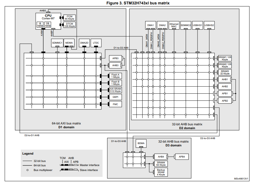
圖1.STM32H743xI框圖
評估板STM32H743I-EVAL
The STM32H743I-EVAL Evaluation board is a high-end development platform for the ARM? Cortex?-M7-based STM32H743XI microcontroller. The STM32H743I-EVAL Evaluation board provides access to all the STM32 peripherals for user applications and includes an embedded ST-LINK debugger/programmer. The full range of the hardware features on the STM32H743I-EVAL Evaluation board, helps to evaluate all the peripherals (USB OTG HS and FS, Ethernet, FD-CAN, USART, Audio DAC and ADC, digital microphone, SRAM, SDRAM, NOR Flash, Twin Quad-SPI Flash, microSD? 3.0 card and 5.7” 640x480 TFT color LCD with touch screen) and to develop applications.
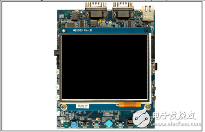
圖2.評估板STM32H743I-EVAL外形圖
評估板STM32H743I-EVAL主要特性:
? STM32H743XIH6 microcontroller with 2 Mbytes of Flash memory and 1 Mbyte of RAM in TFBGA240+25 package
? 5.7” 640x480 TFT-color LCD with touch screen
? Ethernet compliant with IEEE-802.3-2002
? USB OTG HS and FS
? I2C compatible serial interface
? RTC with rechargeable backup battery
? SAI Audio DAC
? ST-MEMS digital microphones
? 8-Gbyte (or more) SDIO3.0 interface microSD? card
? 8Mx32-bit SDRAM, 1Mx16bit SRAM and 8Mx16-bit NOR Flash
? 1 1-Gbit Twin Quad-SPI NOR Flash memory or two 512Mb Quad-SPI NOR Flash memories
? Potentiometer
? 4 colored LEDs
? Reset, wakeup, tamper or key buttons
? Joystick with 4-direction control and selector
? Board connectors
– Power jack
– 3 USB with Micro-AB
– RS-232 communications
– Ethernet RJ45
– FD-CAN compliant connection
– Stereo headset jack including analog microphone input
– 2 audio jacks for external speakers
– microSD? card
– JTAG/SWD and ETM trace
? Board expansion connectors:
– Extension connectors and memory connectors for daughterboard or wire-wrap board
? Flexible power-supply options: ST-LINK USB VBUS or external sources
? On-board ST-LINK/V2-1 debugger/programmer with USB re-enumeration capability: mass storage, virtual COM port and debug port
? Comprehensive free software libraries and examples available with the STM32Cube package
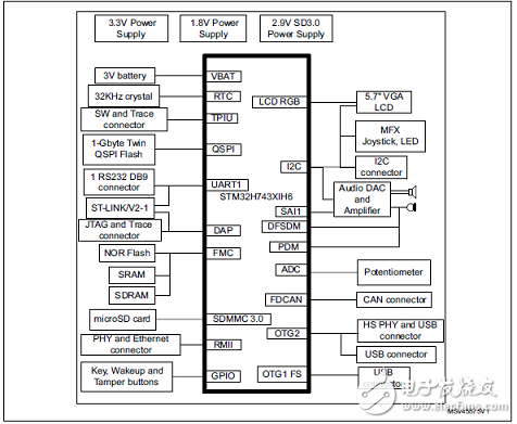
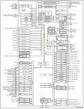
圖3.評估板STM32H743I-EVAL硬件框圖
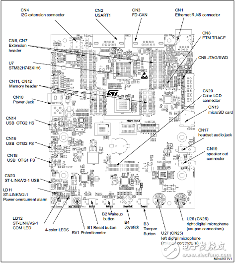
圖4.評估板STM32H743I-EVAL主要元件分布圖
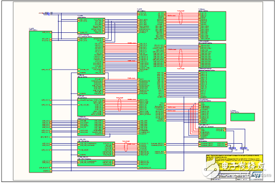
圖5.評估板STM32H743I-EVAL電路圖(1)

圖6.評估板STM32H743I-EVAL電路圖(2):MCU
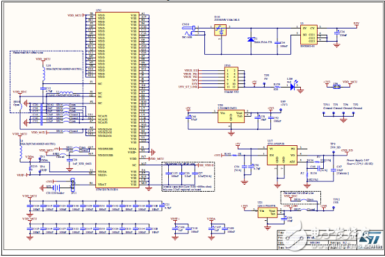
圖7.評估板STM32H743I-EVAL電路圖(3):電源
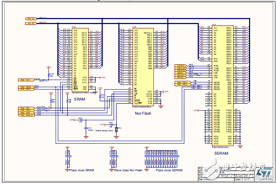
圖8.評估板STM32H743I-EVAL電路圖(4):SRAM,閃存和SDRAM
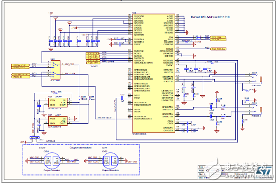
圖9.評估板STM32H743I-EVAL電路圖(5):音頻

圖10.評估板STM32H743I-EVAL電路圖(6):LCD連接器

圖11.評估板STM32H743I-EVAL電路圖(7):以太網(wǎng)

圖12.評估板STM32H743I-EVAL電路圖(8):USB OTG HS
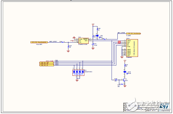
圖13.評估板STM32H743I-EVAL電路圖(9):USB OTG FS
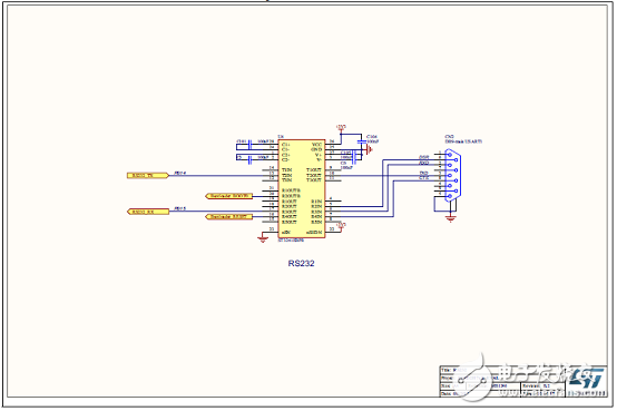
圖14.評估板STM32H743I-EVAL電路圖(10):RS232
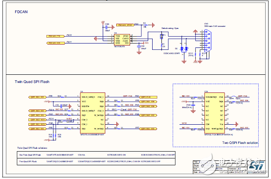
圖15.評估板STM32H743I-EVAL電路圖(11):FDCAN和QSPI
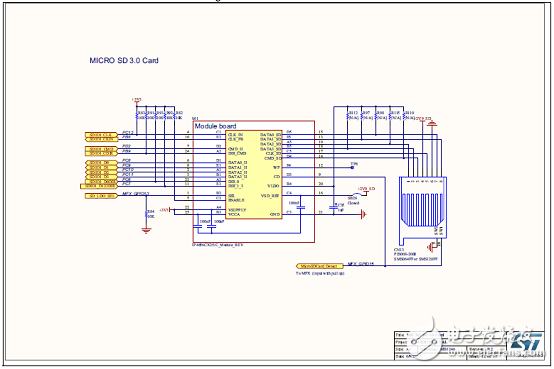
圖16.評估板STM32H743I-EVAL電路圖(12):microSD 3.0卡
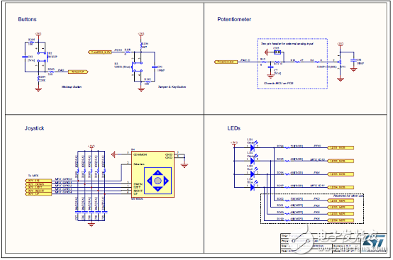
圖17.評估板STM32H743I-EVAL電路圖(13):外設(shè)

圖18.評估板STM32H743I-EVAL電路圖(14):擴展連接器
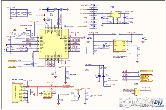
圖19.評估板STM32H743I-EVAL電路圖(15):ST-LINK/V2-1
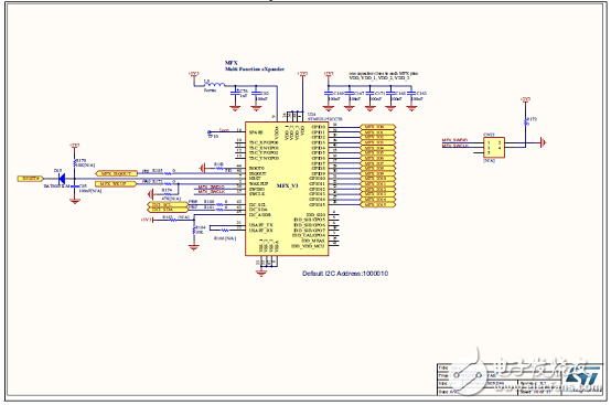
圖20.評估板STM32H743I-EVAL電路圖(16):MFX

圖21.評估板STM32H743I-EVAL電路圖(17):JTAG和跟蹤

圖22.評估板STM32H743I-EVAL電路圖(18):5.7” LCD板
-
mcu
+關(guān)注
關(guān)注
146文章
17918瀏覽量
362760 -
ST公司
+關(guān)注
關(guān)注
1文章
45瀏覽量
32144
發(fā)布評論請先 登錄
ST基于ARM? Cortex?-M7內(nèi)核的STM32H7系列高性能MCU簡介及資料!
電機代碼生成及控制算法——STM32H743模型設(shè)計參數(shù)配置
如何將STM32H743I EVAL板的TX和RX引腳短接在一起呢?
請問CUBEIDE中如何正確配置STM32H743I EVAL2觸摸屏的初始化?
OLIMEX STM32F103 MCU開發(fā)方案
ST STM32L4R9I高性能超低功耗ARM MCU開發(fā)方案
STM32H743XI 32位ARM處理器的數(shù)據(jù)手冊免費下載
微雪電子開發(fā)板CoreH743I STM32H743IIT6簡介
微雪電子開發(fā)板 OpenH743I-C STM32H743IIT6簡介
STM32H743ZGT6 STMicroelectronics STM32H7 高性能MCU
回顧當年的MCU跑分王 STM32H7特性解讀
stm32h7內(nèi)存分配_STM32H7 - ARM Cortex-M7 MCUs (400 MHz) - STMicroelectronics

STM32H743I/F767I核心板開源
STM32H723/733、STM32H725/735 和 STM32H730 超值系列 先進的基于 Arm ? 的 32 位 MCU


 工商網(wǎng)監(jiān)
評論