
| Function | Clock generator |
| Number of outputs | 5 |
| Output frequency (Max) (MHz) | 800 |
| Core supply voltage (V) | 3.3 |
| Output supply voltage (V) | 3.3 |
| Input type | LVCMOS, LVPECL |
| Output type | LVPECL |
| Operating temperature range (C) | -40 to 85 |
| Features | Op-amp for active loop filter, Programmable delay |
| Rating | Catalog |
- High Performance 1:5 PLL Clock Synchronizer
- Two Clock Inputs: VCXO_IN Clock Is Synchronized to REF_IN Clock
- Synchronizes Frequencies up to 800 MHz (VCXO_IN)
- Supports Five Differential LVPECL Outputs
- Each Output Frequency Is Selectable by x1, /2, /4, /8, /16
- All Outputs Are Synchronized
- Integrated Low-Noise OPA for External Low-Pass Filter
- Efficient Jitter Screening From Low PLL Loop Bandwidth
- Low-Phase Noise Characteristic
- Programmable Delay for Phase Adjustments
- Predivider Loop BW Adjustment
- SPI Controllable Division Setting
- Power-Up Control Forces LVPECL Outputs to 3-State at VCC <1.5 V
- 3.3-V Power Supply
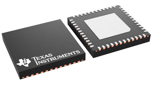
- Packaged In 64-Pin BGA (0,8 mm Pitch - ZVA) or 48-Pin QFN (RGZ)
- Industrial Temperature Range –40°C to 85°C
The CDC7005 is a high-performance, low-phase noise, and low-skew clock synchronizer and jitter cleaner that synchronizes the voltage controlled crystal oscillator (VCXO) frequency to the reference clock. The programmable predividers M and N give a high flexibility to the frequency ratio of the reference clock to VCXO: VCXO_IN/REF_IN = (NxP)/M. The VCXO_IN clock operates up to 800 MHz. Through the selection of external VCXO and loop filter components, the PLL loop bandwidth and damping factor can be adjusted to meet different system requirements. Each of the five differential LVPECL outputs is programmable by the serial peripheral interface (SPI). The SPI allows individual control of frequency and enable/disable state of each output. The device operates in 3.3-V environment. The built-in latches ensure that all outputs are synchronized.
The CDC7005 is characterized for operation from ?40°C to 85°C.


