

| Number of channels (#) | 1 |
| Isolation rating (Vrms) | 5700 |
| Power switch | GaNFET, MOSFET |
| Peak output current (A) | 6 |
| DIN V VDE V 0884-10 transient overvoltage rating (Vpk) | 8000 |
| DIN V VDE V 0884-10 working voltage (Vpk) | 1414 |
| Output VCC/VDD (Max) (V) | 18 |
| Output VCC/VDD (Min) (V) | 6 |
| Input VCC (Min) (V) | 3 |
| Input VCC (Max) (V) | 5.5 |
| Prop delay (ns) | 28 |
| Operating temperature range (C) | -40 to 125 |
| Undervoltage lockout (Typ) | 5 |
- Reinforced isolation
- Single channel in DWV Package with 8.5-mm creepage distance
- CMTI greater than 100-V/ns
- 4-A peak source, 6-A peak sink output
- Switching parameters:
- 40-ns maximum propagation delay
- 5-ns maximum delay matching
- 5.5-ns maximum pulse-width distortion
- 35-μs maximum VDD power-up delay
- Up to 18-V VDD output drive supply
- 5-V VDD UVLO
- Operating temp. range (TA) –40°C to 125°C
- Rejects input pulses shorter than 5-ns
- TTL and CMOS compatible inputs
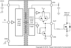
The UCC5304 device is an isolated single-channel gate driver with 4-A peak-source and 6-A peak-sink current. It is designed to drive power MOSFETs and GaNFETs in PFC, Isolated AC/DC, DC/DC, and synchronous rectification applications, with fast switching performance and robust ground bounce protection through greater than 100-V/ns common-mode transient immunity (CMTI).
The UCC5304 is available in a 8.5 mm SOIC-8 (DWV) package and can support isolation voltage up to 5-kVRMS. Compared to an optocoupler, the UCC5304 family has lower part-to-part skew, lower propagation delay, higher operating temperature, and higher CMTI.
Protection features include: IN pin rejects input transient shorter than 5-ns; both input and output can withstand –2-V spikes for 200-ns, both supplies have undervoltage lockout (UVLO), and active pull down protection clamps the output below 2.1-V when unpowered or floated.
With these features, this device enables high efficiency, high power density, and robustness in a wide variety of power applications.


