
| Number of series cells | 1, 2, 3, 4 |
| Charge current (Max) (A) | 5 |
| Operating Vin (Max) (V) | 24 |
| Cell chemistry | Li-Ion/Li-Polymer, Lithium Phosphate/LiFePO4 |
| Battery charge voltage (Min) (V) | 3 |
| Battery charge voltage (Max) (V) | 18.8 |
| Absolute Vin (safety rating) (Max) ((V)) | 30 |
| Control interface | I2C |
| Features | BAT temp thermistor monitoring (JEITA profile), IC thermal regulation, ICO (Input Current Optimization), IINDPM (Input current limit), Input OVP, Integrated ADC, Power Path, USB C/PD compatible, USB D+/D-/BC1.2 integrated, USB OTG integrated, VINDPM (Input voltage threshold to maximize adaptor power) |
| Operating Vin (Min) (V) | 3.6 |
| Rating | Catalog |
- High efficient synchronous Switch Mode buck-boost charger for 1-4 cell battery
- 750-kHz and 1.5-MHz Programmable switching frequencies
- Efficiency optimized for charging 2s battery, 96.5% efficiency with 9-V input and 94.5% efficiency with 15-V input at 3-A ICHG
- Charging current up to 5 A with 10-mA resolution
- Support wide range of input sources
- 3.6-V to 24-V Wide input operating voltage range with 30-V absolute maximum rating
- Maximum power tracking with VINDPM up to 22 V and IINDPM up to 3.3 A
- Detect USB BC1.2, SDP, CDP, DCP, HVDCP and non-standard adapters
- Dual-input power mux controller for source selection
- High level integration
- Four switching MOSFETs and BATFET
- Input current and charging current sensing
- Narrow-VDC (NVDC) Power Path management
- Power USB port from battery (USB OTG)
- 2.8-V to 22-V OTG output voltage with 10-mV resolution to support USB-PD PPS
- OTG Output current regulation up to 3.32 A with 40-mA resolution
- Flexible autonomous and I2C mode for optimal system performance
- Integrated 16-bit ADC for voltage, current and temperature monitor
- Low battery quiescent current
- Typical 21-μA at battery only operation
- Typical 600 nA in Charger Shutdown Mode
- High accuracy
- ±0.5% Charge voltage regulation for 2s battery
- ±5% Charge current regulation
- ±5% Input current regulation
- Safety
- Thermal regulation and thermal shutdown
- Input/battery OVP and OCP
- Converter MOSFETs OCP
- Charging safety timer
- Package
- 56-Pin 2.9mm × 3.3mm WCSP
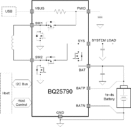
The BQ25790 is a fully integrated switch-mode buck-boost charger for 1-4 cell Li-ion battery and Li-polymer battery. The integration includes 4 switching MOSFETs (Q1, Q2, Q3, Q4), input and charging current sensing circuits, the battery FET (QBAT) and all the loop compensation of the buck-boost converter. It provides high power density and design flexibility to charge batteries across the full input voltage range for USB Type-C? and USB power delivery (USB-PD) applications such as smart phone, tablet and other portable devices.
The charger supports the narrow VDC power path management, in which the system is regulated at a voltage slightly higher than the battery voltage, but not drop below the minimum system voltage. The system keeps operating even when the battery is completely discharged or removed. When load power exceeds input source rating, the battery gets into supplement mode and prevents the input source from being overloaded and the system from crashing.
The device charges a battery from a wide range of the input sources including legacy USB adapter to high voltage USB PD adapter and traditional barrel adapter. The charger automatically sets converter to be buck, boost or buck-boost configurations based on input voltage and battery voltage without the host control. The dual input source selector manages the power flowing from two different input sources. The inputs selection is controlled by the host through I2C with default source #1 (VAC1) as the primary input and the source #2 (VAC2) as the secondary input.
To support fast charging using adjustable high voltage adapter, the device provides D+/D- handshake. The device is compliant with USB 2.0 and USB 3.0 power delivery specification with input current and voltage regulation. In addition, the Input Current Optimizer (ICO) allows the detection of maximum power point of an unknown input source.
Besides the I2C host controlled charging mode, this charger also supports autonomous charging mode. After power up, the charging is enabled with default register settings. The device can complete a charging cycle without any software engagements. It detects battery voltage and charges the battery in different phases: trickle charging, pre-charging, constant current (CC) charging and constant voltage (CV) charging. At the end of the charging cycle, the charger automatically terminates when the charge current is below a pre-set limit (termination current) in the constant voltage phase. When the full battery falls below the recharge threshold, the charger will automatically start another charging cycle.
In the absence of input sources, this device supports USB On-the-Go (OTG) function, discharging battery to generate an adjustable 2.8V~22V voltage on VBUS with 10mV step size, which is compliant to the USB PD 3.0 specification defined programmable power supply (PPS) feature.
The charger provides various safety features for battery charging and system operations, including battery temperature negative thermistor monitoring, trickle charge, pre-charge and fast charge timers and over-voltage/over-current protections on battery and input. The thermal regulation reduces charge current when the junction temperature exceeds a programmable threshold. The STAT output of the device reports the charging status and any fault conditions. The PG output indicates if a good power source is present. The INT pin immediately notifies host when fault occurs.
The device also provides a 16-bit analog-to-digital converter (ADC) for monitoring charge current and input/battery/system (VAC, VBUS, BAT, SYS, TS) voltages.
It is available in a 56-pin 2.9mm × 3.3mm WCSP package.


