| Bus voltage (Max) (V) | 28 |
| Power switch | MOSFET |
| Input VCC (Min) (V) | 4.5 |
| Input VCC (Max) (V) | 15 |
| Peak output current (A) | 2.4 |
| Rise time (ns) | 50 |
| Operating temperature range (C) | -40 to 125 |
| Rating | Catalog |
| Number of channels (#) | 2 |
| Fall time (ns) | 50 |
| Prop delay (ns) | 75 |
| Iq (uA) | 3000 |
| Input threshold | CMOS |
| Channel input logic | CMOS |
| Negative voltage handling at HS pin (V) | 0 |
| Features | Dead Time Control, Synchronous Rectification |
| Driver configuration | Inverting |
- Floating Bootstrap or Ground-Reference High-Side Driver
- Adaptive Dead-Time Control
- 50-ns Max Rise/Fall Times and 100-ns Max Propagation Delay \x96 3.3-nF Load
- Ideal for High-Current Single or Multiphase Power Supplies
- 2.4-A Typical Peak Output Current
- 4.5-V to 15-V Supply Voltage Range
- Internal Schottky Bootstrap Diode
- Low Supply Current....3-mA Typical
- \x9640°C to 125°C Operating Virtual Junction Temperature
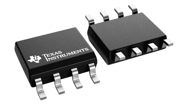
- Available in SOIC Package
The TPS2832 and TPS2833 are MOSFET drivers for synchronous-buck power stages. These devices are ideal for designing a high-performance power supply using switching controllers that do not have MOSFET drivers. The drivers are designed to deliver 2.4-A peak currents into large capacitive loads. The high-side driver can be configured as a ground-reference driver or as a floating bootstrap driver. An adaptive dead-time control circuit eliminates shoot-through currents through the main power FETs during switching transitions and provides high efficiency for the buck regulator.
The TPS2832 has a noninverting input. The TPS2833 has an inverting input. The TPS2832/33 drivers, available in 8-terminal SOIC packages, operate over a junction temperature range of \x9640°C to 125°C.


