 電子發燒友App


LDO也就是線性穩壓電路,從應用的輸入電壓中減去超額的電壓,產生經過調節的輸出電壓。LDO(低壓降)穩壓器通常使用功率晶體管(也稱為傳遞設備)作為 PNP。本文將淺談一下關于模擬電路應用之LDO的PSRR計算。
講講作者君最近有見過的一個很基本的電路:LDO(A low-dropout or LDO regulator is a DC linear voltage regulator that can regulate the output voltage even when the supply voltage is very close to the output voltage.),就是傳說中的無處不在的穩壓電路。

作者君搗鼓這個電路的初衷,是看看我調整了input電壓之后,PSRR有沒有很顯著的惡化。因為之前有個別人做好的LDO,但是input是bandgap的1.2V,作者君把input改成0.8V之后,就稍微改了一些東西:比如把之前OTA的input pair從pmos變成了nmos。然后,因為這個LDO的PSRR要求比較高,作者君就小小的搗鼓了一下PSRR的計算。
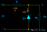
我們還是從書本來說起吧!
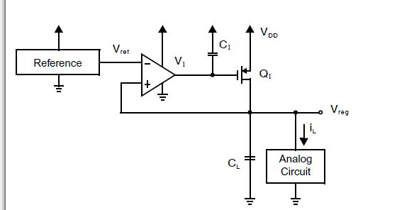
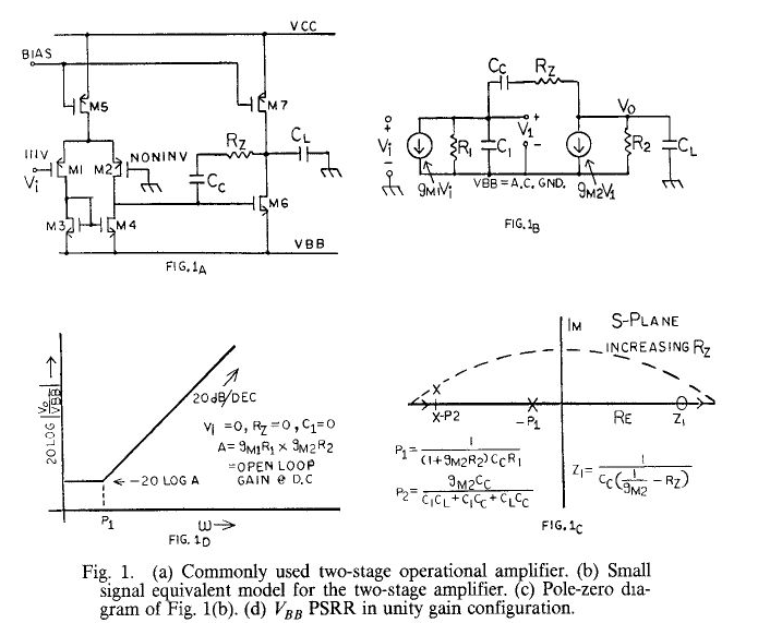
上面的圖是來自“Analog Integrated Circuit Design, 2nd Edition,Tony Chan Carusone, David Johns, Kenneth Martin”
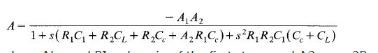
不管怎么說,我們要考慮一個系統的frequency response特性,首先跑不掉的就是loop gain。 因此,可以按照下面的公式算出loop gain,其中包括兩個可以預計到的pole:一個在OTA的output,一個在LDO的output:
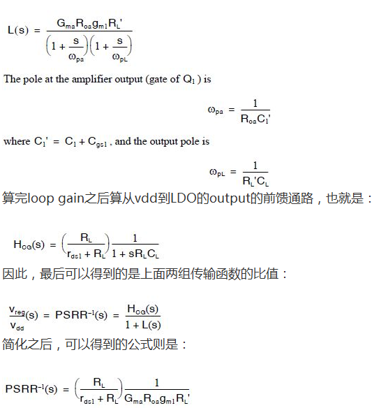
可以看出,DC時候的PSRR其實就是整個system的DC gain的一部分。因此,想得到一個大的PSRR,需要有一個比較大的gain的OTA,這個是可以預料到的。
同時,如果我們考慮上面兩個都可以成為主極點的pole的大小,可以用下面的圖來解釋。
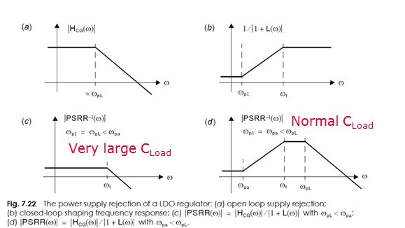
圖a是PSRR公式里面的分子部分,也就是前饋部分。然后,圖b是分母部分,也就是整個system的loop gain。
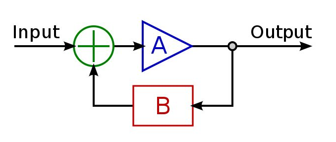
或者說,分子就是這個經典feedback system里面的A,就是從VDD到output的傳輸函數;然后分母是AB,就是loop gain。
因此,考慮兩種不同的情況:LDO的輸出是主極點,就得到了圖c;OTA的output 是主極點,就得到了圖d。
大家應該可以再次感受到了用dB做單位的好處:PSRR的公式就是直接把圖a和圖b相加的結果!多么簡單直觀啊!
然后,這樣一來,作者君發現:可以用PSRR來判斷哪個pole是主極點!OTA的輸出是主極點時,PSRR是圖d;而LDO的output是主極點的時候,PSRR是圖c!哼哼!這樣算是“一物多用”嗎?
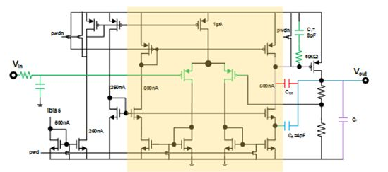
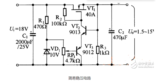
作者君的實際電路是下面這樣子的。
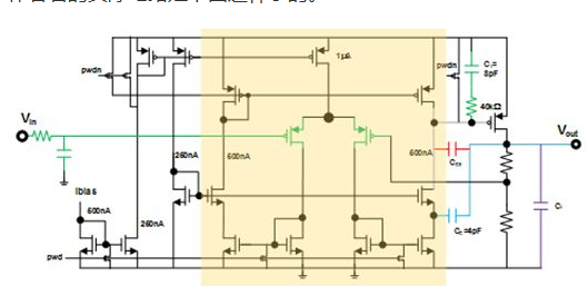
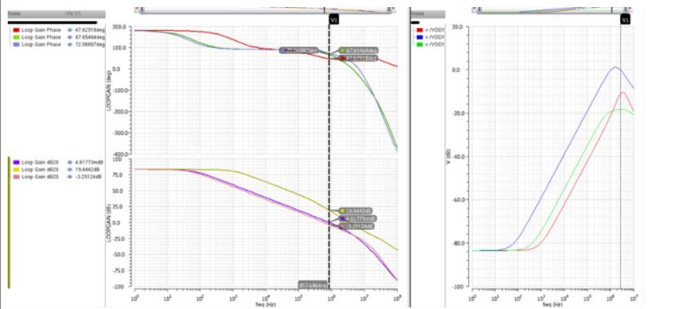
陰影部分就是OTA。如果compensation capacitor只有下圖里面紅色的miller capacitor Cc0和紫色的CL時,我調整了一下CL的大小,PSRR的simulation results如下圖:
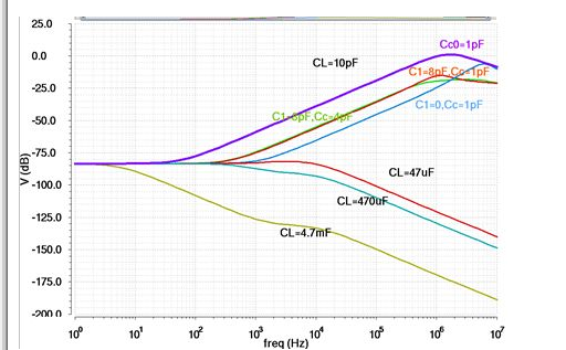
也就是說,想要得到上面那張圖7.22(C)里面的完全不向上翹起的結果,你的CL必須相當大。比如,CL要47uF。而此時,miller capacitor才不過1pF而已……大家感受一下數量級的差距。因此,若是有條件接片外電容,大家放心大膽的用。但是若是只能用片上的電容,大家就得小心一些了。
比如:看看大約在1MHz左右,最上面那條紫色的線,居然超過0dB了!也就是說,VDD上面的高頻擾動會被放大之后顯現在LDO的output上面!
因此,其實作者君拿到的LDO并不是用紅色的Cc0來做compensation的,而是加上了藍色的Cc和綠色的C1。這樣一看,OTA的output node(或者說是輸出級的power pmos的gate)并沒有通過capacitor連接起來。而是,跨過了一個common gate的nmos,Cc才連著output那里。
然后,作者君就找到了這個傳說中的著名AHUJA compensation的paper:An Improved Frequency Compensation Technique for CMOS Operational Amplifiers, BHUPENDRA K. AHUJA, IEEE JOURNAL OF SOLID-STATE CIRCUITS, VOL. SC-18,NO. 6, DECEMBER 1983, p629
不好意思,抄一點paper的原文,因為本人覺得自己寫的不會更好……
這個傳統的miller compensation的問題有兩個:
無法驅動很大的電容負載:The op amp stability is severely degraded for capacitive loads of the same order as compensation capacitor (CL must be less than gM2CC/g~l to avoid second pole crossover of the unity gain frequency)。
當power mos是nmos的時候,miller造成的zero會嚴重影響PSRR的性能:In case of p-channel MOS transistors for the input differential stage, the negative power supply displays a zero at the dominant pole frequency of the op amp in unity gain configuration. This results in serious performance degradation for sampled data systems which use high-frequency switching regulators to generate their power supplies. (In the case of n-channel MOS transistors for the input differential pair, it is the positive supply which shows similar degradation.) This is illustrated in Fig. l(d)。
然后,這個compensation的idea就是除去這個可以short第一級output和第二級output。下面的內容大家不想看可以略去。
The technique is based on removing the feed forwardpath from the first stage output to the op amp output. The circuit shown in Fig. 1 has a current CCd(V. – Vl)/dt flowing into the first-stage output. If one can devise a circuit where only CCdVO/dt current flows into the first stage output, one would have eliminated the feedforward path while still producing a dominant pole due to the Miller effect. The only difference is that Miller capacitance is now AICCrather than (1+ AZ) CCwhere A~is the secondstage voltage gain. Thus, the conceptual ac equivalent of such a circuit is shown in Fig. 2(a)。 Here the compensation capacitor is shown to be connected between the output node and a virtual ground (or ac ground), while the controlled current source having the same value as CCdVo/dt charges the first-stage output. It can be shown that for such an arrangement, the open-loop gain of the op amp is given by
where Al = g~l RI = dc gain of the first stage and A2 = gm2Rz = clc gain of the second stage.
Fig. 2(b) shows its pole-zero location. Notice that there is no finite zero in this circuit and that both the poles are real and are widely spaced.
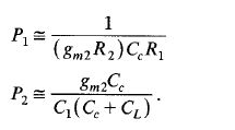
Assuming the internal node capacitance Cl being much smaller than the compensation capacitor CCor the load capacitance CL, the unity gain frequency WI is still given by g~l/CC. This results in
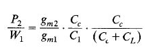
Taking some typical design values of a two-stage amplifier as given by
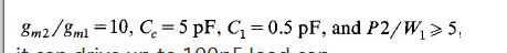
it can drive up to 100pF load cap.
another advantage is:
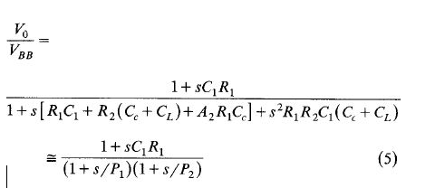
which indicates that is has the same poles as the open-loop gain and a zero which is created by the parasitic capacitance at the first-stage output. Thus, in a unity gain configuration, the VBB PSRR is given by
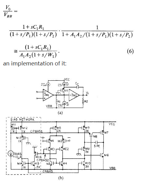
重新貼一下我的電路:
A: nomarl miller (direct,紅色Cc0), 1.5pF
B: modified miller (indirect,藍色Cc和綠色C1): 8pF and 4pF
最后比較了一下使用這個compensation之后的PSRR:果然可以很顯著的把1MHz那里的peak壓下去。比如綠色的那根線,peak被壓到了-20dB了。
我們還可以再確認一下,到底dominant pole是不是在那個compensation cap的左邊(或者已經可以從PSRR看出來),作者君又改了一下那個Cc的值,得到了下面的loop gain:Cc=0.4pF or 4pF:
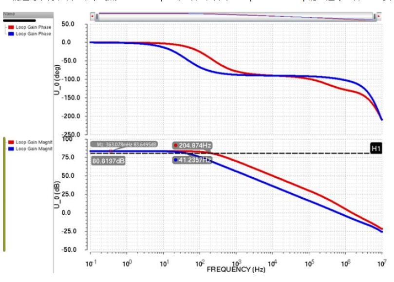
當把Cc從4pF(藍色)變成0.4pF(紅色)之后,明顯看到dominant pole往外移動了。


 工商網監
工商網監
評論