 基于UCC21225A隔離雙路柵極驅動和參考設計
TI公司的ucc21225A是隔離雙路柵極驅動器,具有源電流4A和沉峰值電流6A,封裝為5-mm x 5-mm LGA-13.可以驅動高達5MHz的功率晶體管,具有業界最低的時延和脈寬失真。典型的傳輸時延為19ns,最大時延匹配為5ns,脈寬失真最大為6ns.兩個次級邊驅動器間內部功能隔離允許工作電壓高達700V,可配置成兩個低邊,兩個高邊,或有可編死區時間(DT)的半橋驅動器,器件的VDD電源電壓高達25V,寬輸入VCCI范圍從3V到18V,使得驅動非常適合于模擬和數字控制器間的接口,所有的電源引腳有欠壓鎖住(UVLO)保護。相關的安全規范包括3535-VPK Isolation per DIN V VDE V 0884-11:2017-01和2500-VRMS Isolation for 1 Minute per UL 1577.主要用在服務器,通信,IT和工業領域,DC/DC轉換器和AC/DC轉換器,馬達驅動和DC/AC太陽能逆變器以及HEV和BEV電池充電器。本文介紹了UCC21225A主要特性,框圖和功能框圖,典型應用電路圖以及10kW三級三相連接電網的太陽能逆變器參考設計TIDA-0160610-kW主要特性和指標,框圖,電路圖和材料清單。
The UCC21225A is an isolated dual-channel gatedriver with 4-A source and 6-A sink peak current in a5-mm x 5-mm LGA-13 package. It is designed todrive power transistors up to 5-MHz with best-in-classpropagation delay and pulse-width distortion.
The input side is isolated from the two output driversby a 2.5-kVRMS isolation barrier, with 100-V/nsminimum common-mode transient immunity (CMTI)。
Internal functional isolation between the twosecondary side drivers allows working voltage up to700-VDC.This driver can be configured as two low-side, twohigh-side, or a half-bridge driver with programmabledead time (DT)。 A disable pin shuts down bothoutputs simultaneously when it is set high, and allowsnormal operation when left open or grounded.
The device accepts VDD supply voltages up to 25-V.A wide input VCCI range from 3-V to 18-V makes thedriver suitable for interfacing with both analog anddigital controllers. All the supply voltage pins haveunder voltage lock-out (UVLO) protection.
With all these advanced features, the UCC21225Aenables high power density, high efficiency, androbustness in a wide variety of power applications.
UCC21225A主要特性:
1? Universal: Dual Low-Side, Dual High-Side or Half-Bridge Driver
? 5 x 5 mm, Space-Saving LGA-13 Package
? Switching Parameters:
– 19-ns Typical Propagation Delay
– 5-ns Maximum Delay Matching
– 6-ns Maximum Pulse-Width Distortion
? CMTI Greater than 100-V/ns
? 4-A Peak Source, 6-A Peak Sink Output
? TTL and CMOS Compatible Inputs
? 3-V to 18-V Input VCCI Range
? Up to 25-V VDD with 5-V UVLO
? Programmable Overlap and Dead Time
? Rejects Input Transients Shorter than 5-ns
? Fast Disable for Power Sequencing
? Safety-Related Certifications:
– 3535-VPK Isolation per DIN V VDE V 0884-11:2017-01
– 2500-VRMS Isolation for 1 Minute per UL 1577
– CQC per GB4943.1-2011 (Planned)
UCC21225A應用:
? Server, Telecom, IT and Industrial Infrastructures
? DC-DC and AC-to-DC Power Supplies
? Motor Drive and DC-to-AC Solar Inverters
? HEV and BEV Battery Chargers

圖1. UCC21225A框圖

圖2. UCC21225A功能框圖
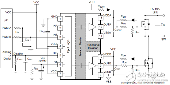
圖3. UCC21225A典型應用電路圖
10kW三級三相連接電網太陽能逆變器的參考設計TIDA-0160610-kW
This reference design provides an overview on how toimplement a three-level, three-phase, SiC-basedDC/AC grid-tie inverter stage. A higher switchingfrequency of 50 kHz reduces the size of magnetics forthe filter design and as a result a higher power density.SiC MOSFETs with switching loss ensures higher DCbus voltages of up to 1000 V and lower switchinglosses with a peak efficiency of 99%. This design isconfigurable to work as a two-level or three-levelinverter.
參考設計TIDA-0160610-kW主要特性:
? Rated Nominal and Max Input Voltage at 800-Vand 1000-V DC
? Max 10-kW/10-kVA Output Power at 400-V AC50- or 60-Hz Grid-Tie Connection
? Operating Power Factor Range From 0.7 Lag to0.7 Lead
? High-Voltage (1200-V) SiC MOSFET-Based Full-Bridge Inverter for Peak Efficiency of 98.5%
? Compact Output Filter by Switching Inverter at50 kHz
? 《2% Output Current THD at Full Load
?Isolated Driver ISO5852S With Reinforced Isolationfor Driving High-Voltage SiC MOSFET andUCC5320S for Driving Middle Si IGBT
? Isolated Current Sensing Using AMC1301 for LoadCurrent Monitoring
? TMS320F28379D Control Card for Digital Control
參考設計TIDA-0160610-kW應用:
? Solar String Inverters
? Solar Central Inverters
圖4.參考設計TIDA-0160610-kW外形圖
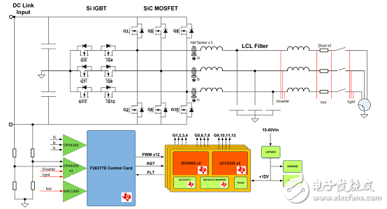
圖5.參考設計TIDA-0160610-kW框圖
參考設計TIDA-0160610-kW主要指標:


圖6.二級三相逆變器架構圖

圖7.二級單相逆變器腿圖

圖8.三級T型三相逆變器架構圖

圖9.參考設計TIDA-0160610-kW電路圖(1):逆變器柵極驅動器
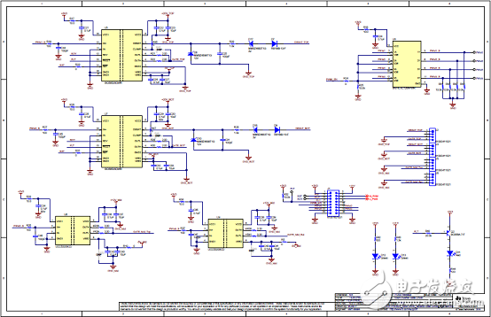
圖10.參考設計TIDA-0160610-kW電路圖(2):逆變器柵極驅動器

圖11.參考設計TIDA-0160610-kW電路圖(3):ISO HV卡

圖12.參考設計TIDA-0160610-kW電路圖(4):ISO HV卡

圖13.參考設計TIDA-0160610-kW電路圖(5):ISO HV卡

圖14.參考設計TIDA-0160610-kW電路圖(6):電源控制卡

圖15.參考設計TIDA-0160610-kW電路圖(7):電源控制卡

圖16.參考設計TIDA-0160610-kW電路圖(8):電源控制卡
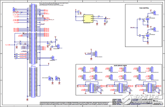
圖17.參考設計TIDA-0160610-kW電路圖(9):電源控制卡
-
晶體管
+關注
關注
77文章
9979瀏覽量
140677 -
柵極驅動
+關注
關注
8文章
208瀏覽量
23540
發布評論請先 登錄
電源和電機驅動的兩種MOS的冗余驅動線路
UCC21225A 采用 LGA 封裝的 4A/6A 2.5kVRMS 隔離式雙通道柵極驅動器
具有高噪聲抗擾度的 UCC21220、UCC21220A 4A/6A雙通道基本隔離式和功能隔離式柵極驅動器數據表

LGA中的4-A、6-A、2.5kVRMS隔離雙通道柵極驅動器UCC21225A數據表
UCC23113 具有功能隔離 (1.2kVRMS) 的 4A/5A 單通道光兼容隔離式柵極驅動器數據手冊
UCC5390-Q1 汽車級 17-A 5kv RMS 單通道隔離式柵極驅動器數據手冊


 工商網監
工商網監
評論