") 功率器件嵌入PCB技術(shù)介紹
功率器件嵌入PCB技術(shù)介紹

最近看到功率器件嵌入PCB的應(yīng)用,了解了一下,感覺(jué)很有前景。照這個(gè)趨勢(shì),將來(lái)會(huì)以PCB封裝各種芯片、被動(dòng)器件,控制器逐漸器件化,整個(gè)供應(yīng)鏈縮短,控制器公司轉(zhuǎn)變?yōu)镻CB級(jí)芯片公司,需求量會(huì)大量減少。要不去整機(jī)廠,要不去搞封裝,感覺(jué)又一波失業(yè)。不過(guò)應(yīng)該對(duì)工藝要求很高,到批量還需要時(shí)間。有沒(méi)有這樣的工作機(jī)會(huì),盡快找一個(gè)為未來(lái)十年積累一點(diǎn)資本。
一、緯湃科技《PCB嵌入式功率模塊技術(shù)走勢(shì)分析和應(yīng)用前景》
印刷電路板(PCB)天然具有以下優(yōu)異的電氣性能:PCB可以進(jìn)行多層布線,通過(guò)控制線間距及層間距減少EMC的影響,絕緣材料可以滿(mǎn)足400~1000V高壓絕緣的要求,并且埋入PCB的電子器件可以通過(guò)高散熱材料和合理的散熱層設(shè)計(jì)達(dá)到優(yōu)秀的散熱性能。這些性能優(yōu)勢(shì)使得PCB嵌入功率芯片技術(shù)用于功率模塊封裝設(shè)計(jì)具有極大的性能潛力。
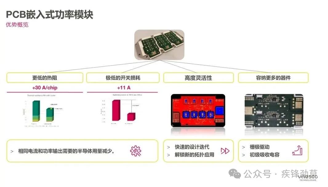
通過(guò)技術(shù)評(píng)估,我們認(rèn)為相較于傳統(tǒng)封裝形式,PCB嵌入式功率模塊單位半導(dǎo)體的通流能力可以提升約40%,或者同樣電流輸出使用的半導(dǎo)體用量減少1/3。同樣功率輸出條件下,功率模塊物料成本有望降低20%。
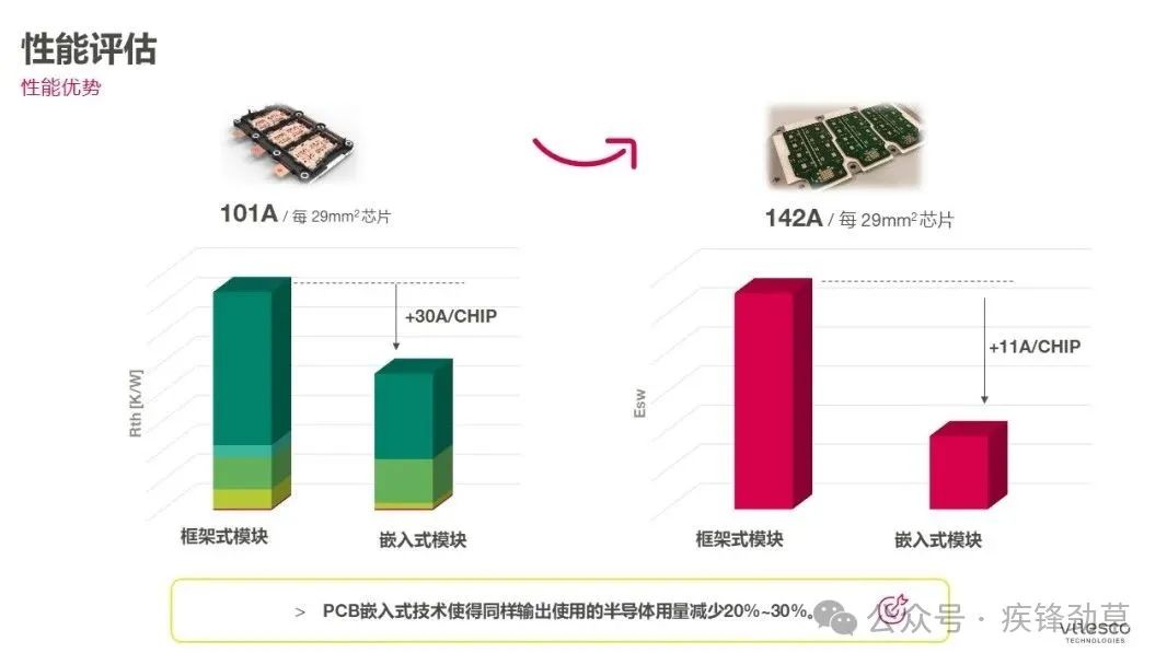
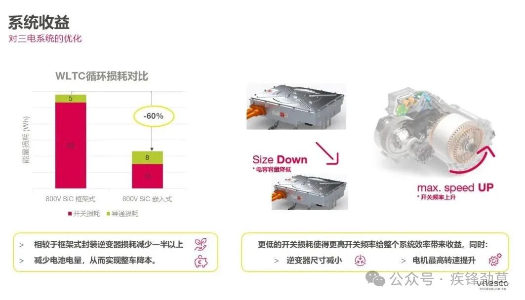
由于新型封裝的功率換流回路雜感可降低到1nH以下,使得逆變器的整體開(kāi)關(guān)損耗降低到原有逆變器產(chǎn)品的1/3,從而開(kāi)關(guān)頻率的提升所帶來(lái)的開(kāi)關(guān)損耗的增加相對(duì)于傳統(tǒng)逆變器降低了2/3。 整車(chē)上可以通過(guò)提高開(kāi)關(guān)頻率來(lái)提升電驅(qū)系統(tǒng)整體的效率,從而基于同樣的續(xù)航里程減少了電池的用量,最終達(dá)到整車(chē)降本的目的。同時(shí)更高的開(kāi)關(guān)頻率使得更小的逆變器體積,以及同樣極對(duì)數(shù)下控制更高速的電機(jī)成為可能。
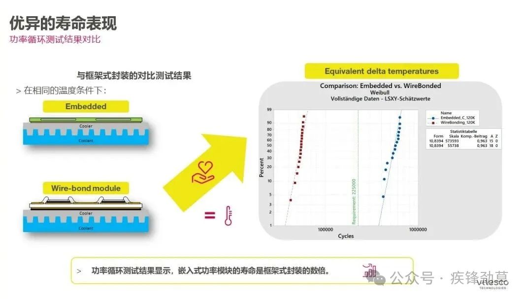
基于目前樣品進(jìn)行的AQG324關(guān)鍵可靠性驗(yàn)證表明,PCB嵌入式封裝的設(shè)計(jì)壽命可達(dá)傳統(tǒng)封裝的數(shù)倍。 基于這一結(jié)果,緯湃科技做了一定的探索,測(cè)試PCB材料對(duì)功率芯片的高工作結(jié)溫的耐受,PCB對(duì)不同工況下的溫度變化的耐受,以及PCB工作在高電壓大電流工況下的絕緣性能等。緯湃科技發(fā)揮多年來(lái)在傳統(tǒng)封裝設(shè)計(jì)中積累的經(jīng)驗(yàn),攻克多種技術(shù)挑戰(zhàn),最終將完成PCB嵌入式功率模塊的產(chǎn)業(yè)化。
https://mp.weixin.qq.com/s/HZMsUVoGpSz_B4oF_lbWfA
二、2024年5月麥格納在USA CTI
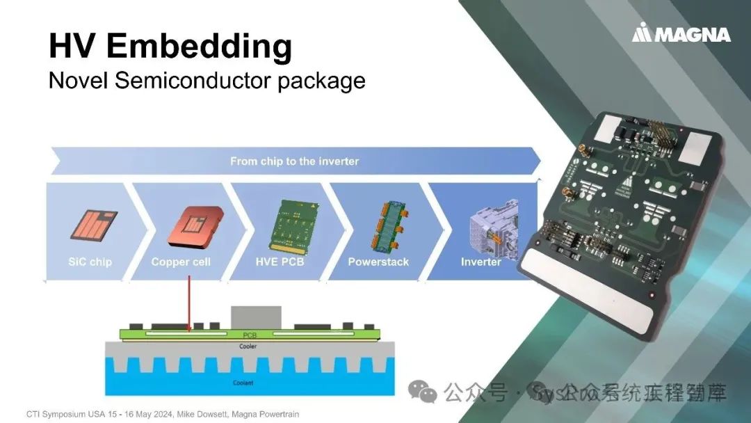
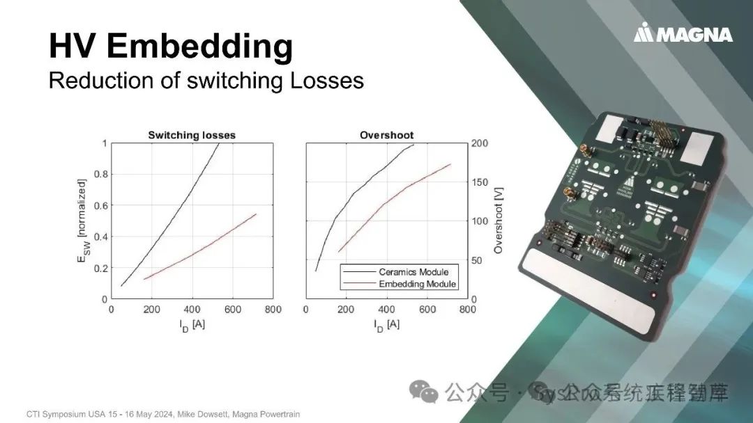
https://mp.weixin.qq.com/s/hS9qpSWBojdSRGcZKxauNw
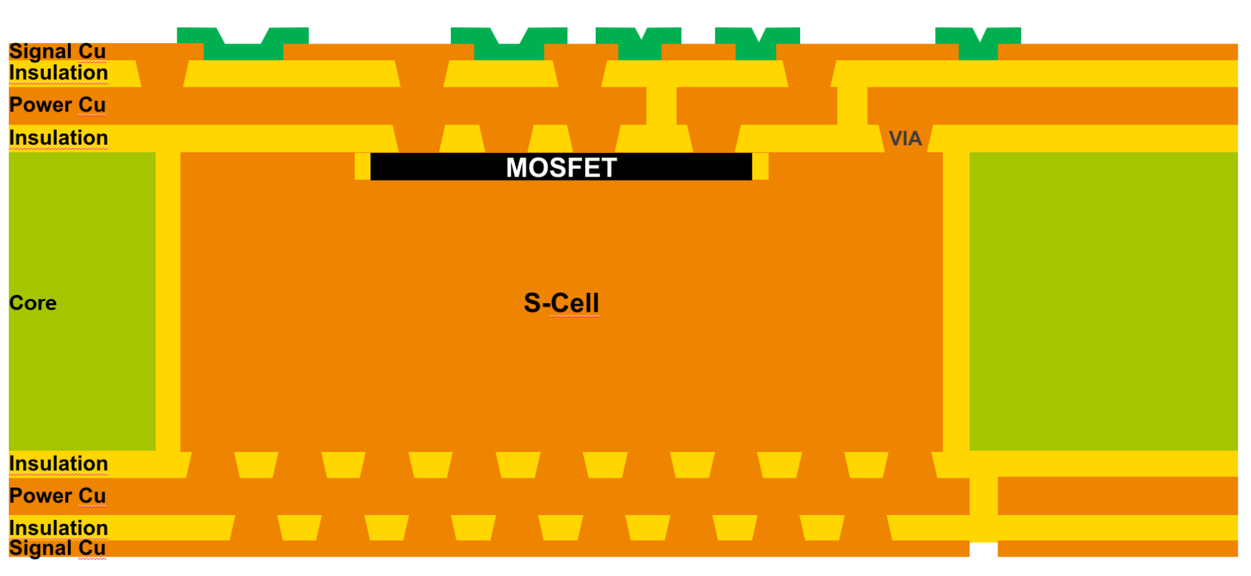
三、英飛凌和 Schweizer Electronic合作片
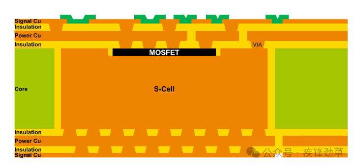
Infineon’s S-Cell 1200 V CoolSiC Gen2p chips
SCHWEIZER 出品的(智能)p2 封裝是一種將功率半導(dǎo)體嵌入印制電路板的技術(shù)。這種方法不僅僅是一種新封裝方法。確切而言,其作用是能根據(jù)完全不同的原理來(lái)研發(fā)電力電子系統(tǒng)。利用智能 p2 封裝技術(shù)研發(fā)的應(yīng)用可實(shí)現(xiàn)高功率、緊湊結(jié)構(gòu)形式和高集成深度。系統(tǒng)供應(yīng)商的制造鏈以及系統(tǒng)中的構(gòu)建和連接技術(shù)都明顯得以簡(jiǎn)化。此外,從系統(tǒng)層面也開(kāi)始有了節(jié)省成本的潛力。
熱阻更低
由于系統(tǒng)中的電感更小,因此開(kāi)關(guān)損耗更低
靜態(tài)情況下的傳導(dǎo)損耗更低
可實(shí)現(xiàn)更高功率密度,因此對(duì)硅的需求更小
明顯提高產(chǎn)品的堅(jiān)固性和使用壽命
如下視頻中介紹p2 封裝信息
schweizer.ag/fileadmin/user_upload/P2_Pack_Full_V3-720p.mp4
文章《Advancing Electric Vehicles with Innovative Chip Embedding and Driver Technology》報(bào)道了測(cè)試性能。Infineon-Chip_Embedding_for_Silcon_Carbide-Article-v01_00-EN.pdf
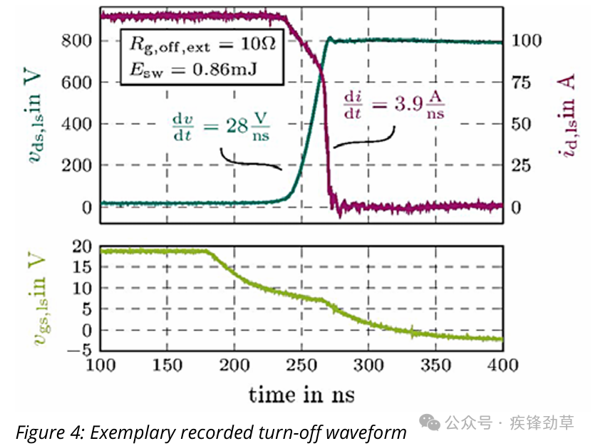
Double pulse measurements In figure 4 a recorded turn-off waveform can be seen. The board was operated at room temperature with a turn-off resistance of 10Ω and a DC link voltage of 800V. The switched off current is 114A. The top graph shows the measured drain current id,ls and drain-source voltage vds,ls of the low-side MOSFET. The lower graph depicts the gate-source voltage vgs,ls. The gate voltage shows a very smooth shape, first discharging the input capacitance. Then as the drain-source voltage starts to rise the miller plateau can be seen. The current reduction in this phase is due to the discharging of the high-side MOSFET during the voltage rise of vds,ls. After forward biasing the high-side body diode the current decreases rapidly. Due to the low inductive design (~2nH) of the switching cell the magnitude of voltage overshoot is minimal. Also, ringing is very low, facilitating to reach EMI targets in the drivetrain. With the demonstrator board, measurements of up to 100 V/ns (turn-off) and 28 A/ ns (diode turn-off) are performed showing no inherent limitations from Infineon’s CoolSiC technology.
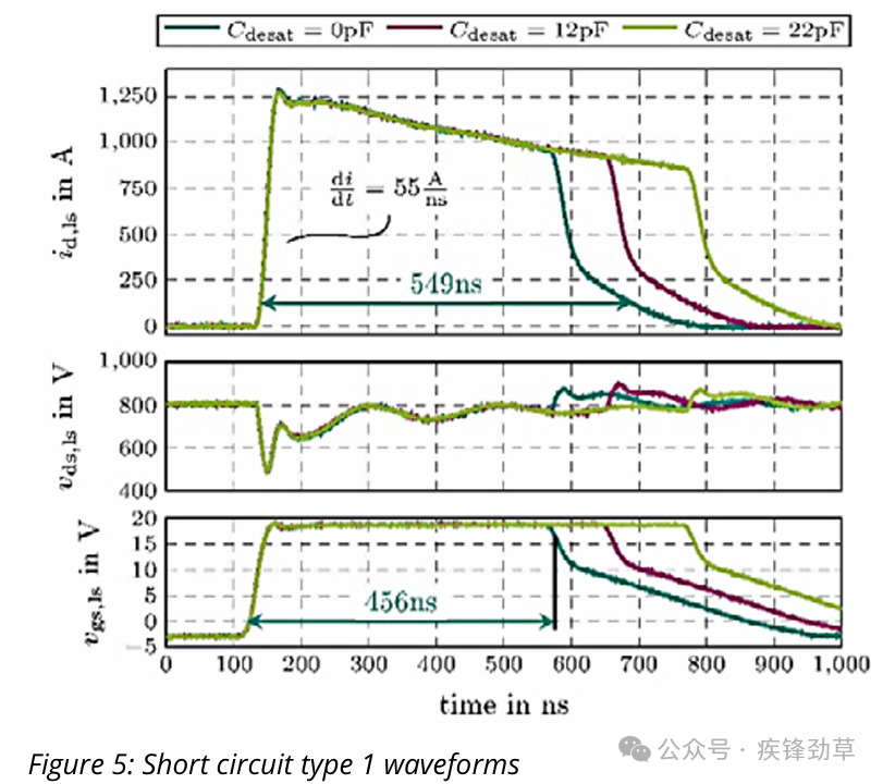
Short circuit measurements and DESAT detection The designed measurement board is also used to test the short circuit behavior of the 1200 V CoolSiC Gen2p under very low-inductive and fast-switching applications. As the shunt resistor cannot withstand the high pulse energy in a short circuit event, it is removed and replaced with a copper sheet. This copper sheet is soldered to the pads of the shunt resistor so that a Rogowski coil can be used. The 3rd generation EiceDRIVER features very low blanking (ideal for SiC), detection and reaction times for the inbuilt DESAT functionality. Measured waveforms can be seen in figure 5. The top figure shows the current for different desaturation capacitors, while the middle and bottom graphs show the drain-source voltage and gate-source voltage. Following a very fast current-rise of 55 A/ns(Rg,on,ext = 0Ω) the current saturates at around 1200 A. Subsequently, the self-heating effect can be seen leading to a reduced saturation current, before turning off the MOSFET via the SOFTOFF pin. It takes the driver only 456 ns after the turn-on (VEE+1.5V) of the driver stage to detect and react (VCC -1.5 V) to the short circuit event. A minimum short circuit time of 549 ns (according to [5]) is reached, showing the striking performance of the combination of an Infineon EiceDRIVER together with an embedded solution. Despite high peak power, the energy reached with the setup is far below the destruction energy of the chip.
四、淺談面向高功率模塊及系統(tǒng)級(jí)封裝(SiP)模塊的新一代芯片嵌入技術(shù)
半導(dǎo)體封裝丨淺談面向高功率模塊及系統(tǒng)級(jí)封裝(SiP)模塊的新一代芯片嵌入技術(shù)
-
pcb
+關(guān)注
關(guān)注
4362文章
23458瀏覽量
408361 -
功率器件
+關(guān)注
關(guān)注
42文章
1927瀏覽量
92477
原文標(biāo)題:功率器件嵌入PCB技術(shù)
文章出處:【微信號(hào):芯長(zhǎng)征科技,微信公眾號(hào):芯長(zhǎng)征科技】歡迎添加關(guān)注!文章轉(zhuǎn)載請(qǐng)注明出處。
發(fā)布評(píng)論請(qǐng)先 登錄
碳化硅功率器件的特性和應(yīng)用
SiC碳化硅MOSFET功率器件雙脈沖測(cè)試方法介紹
碳化硅功率器件的封裝技術(shù)解析
功率器件熱設(shè)計(jì)基礎(chǔ)(十二)——功率半導(dǎo)體器件的PCB設(shè)計(jì)

PCB嵌入式功率芯片封裝,從48V到1200V
功率器件熱設(shè)計(jì)基礎(chǔ)(十一)——功率半導(dǎo)體器件的功率端子
功率半導(dǎo)體嵌入PCB綜述
功率器件嵌入PCB技術(shù)文章分享
功率器件封裝新突破:納米銅燒結(jié)連接技術(shù)
原子層鍍膜在功率器件行業(yè)的應(yīng)用
碳化硅功率器件的技術(shù)優(yōu)勢(shì)
功率地和信號(hào)地pcb怎么處理呢
如何通過(guò)創(chuàng)新封裝技術(shù)提升功率器件性能
探究電驅(qū)動(dòng)系統(tǒng)中碳化硅功率器件封裝的三大核心技術(shù)


 工商網(wǎng)監(jiān)
評(píng)論