") PCB設(shè)計(jì)是可以沒有“地平面”的
PCB設(shè)計(jì)是可以沒有“地平面”的
前面3篇關(guān)于去耦電容的文章引起了很多硬件工程師的興趣,這期的直播課程中講述了“電源、地、去耦電容”,感覺很多網(wǎng)友對(duì)于在PCB設(shè)計(jì)中如何處理“地”一樣是一頭霧水,網(wǎng)上太多的經(jīng)驗(yàn)貼其實(shí)都讓人消化不良,我覺得有必要對(duì)PCB上對(duì)“地”的處理再補(bǔ)充說明一下。
用KiCad軟件對(duì)“地”的處理
正好看到Allaboutcircuits網(wǎng)站上的一篇比較通俗易懂的相關(guān)文章,在這里借花獻(xiàn)佛分享給大家。我一向主張硬件工程師應(yīng)該盡快掌握專業(yè)英語的閱讀,因此這篇文章我就原文貼在這里,我個(gè)人以要點(diǎn)匯總的方式做一下點(diǎn)評(píng)。
以下是作者的原文,藍(lán)色的部分為我的摘要
PCB Layout Tips and Tricks: Use a Ground Plane Whenever Possible
July 11, 2018byRobert Keim
I don’t deny that it is possible to design a PCB without a ground plane, and in many cases you can create a fully functional board this way (or at least it will be fully functional when operating in a favorable environment). But ground planes are an easy way to improve performance and prevent problems, and in my opinion there are few situations in which it is a good idea to make ground connections using ordinary traces.
--作者認(rèn)為PCB設(shè)計(jì)是可以沒有“地平面”的,尤其是在一些比較寬松的環(huán)境下沒有地平面,板子也能夠很好地工作,但如果要提升性能、防止出現(xiàn)問題,地平面是比較簡(jiǎn)單的方式,在作者看來,只有很少的情況才會(huì)只是用普通的走線(Trace和Track都是板子上走線的意思)來進(jìn)行“地”的連接。
Copper Is a Resistor
Schematic diagrams have wires, but in real life there are no wires (unless someone has started manufacturing PCBs using superconductors...). Physical interconnects, including PCB traces, are low-value resistors. The fact that we can often ignore this interconnect resistance doesn’t mean that it has no effect on the functionality of a circuit. On page 8 ofthis documentpublished by Analog Devices, the author demonstrates that a 5 cm PCB trace can introduce over 1 LSb of error in the digitized values generated by a 16-bit ADC.
-- 我們?cè)韴D上的連線都是理想的信號(hào)連接(只是“線”),在實(shí)際的生活中是不存在的,任何物理連接,包括PCB上的走線,都是有比較低的阻抗的,在多數(shù)情況下我們可以忽略低阻抗產(chǎn)生的效應(yīng),但是在有些場(chǎng)合它們可能會(huì)對(duì)電路的功能產(chǎn)生顯著的影響。ADI公司曾證明了5cm長(zhǎng)的PCB走線可能會(huì)導(dǎo)致16位ADC的量化結(jié)果中引入超過1LSb的誤差。
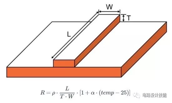
PCB上走線導(dǎo)致的電阻
In many cases there is not much we can do to mitigate the effects of resistance in a signal trace: tiny ICs and the desire for circuit miniaturization often lead to crowded layouts that don’t allow for wide traces or optimal component placement. We can, however, improve the overall situation by using a ground plane, which reduces the resistance of the return path.
-- 很多情況下我們無法減少這些走線電阻帶來的影響,現(xiàn)在的板子越來越小型化,器件也越來越小,所以擁擠的板子上不允許較寬的走線以及非常充裕的空間讓你擺放器件到最佳的位置,在這種情況下,“接地平面”就可以通過為信號(hào)回路提供非常低的阻抗來改善整體的性能。
This decreased return-path resistance is a fundamental benefit of incorporating a ground plane into your PCB. It reduces noise caused by variations in return current, and it establishes a more uniform ground voltage (because less resistance means less voltage being dropped between physically separated portions of the ground net). By dedicating an entire layer to ground and connecting everything to the plane using vias and through-holes, you are making your physical circuit more like the idealized circuit in the schematic diagram.
-- 在PCB設(shè)計(jì)中采用接地平面最大的好處就是能夠降低回路阻抗,它降低了返回電流變化引起的噪聲,在整個(gè)板子上也會(huì)有更均勻的接地電壓(低阻抗意味著較低的壓降),如果整個(gè)層用做“接地平面”,通過過孔(via)或通孔將相關(guān)的電源等連接到接地平面上,物理的電路工作起來就非常接近原理圖了。
Simpler and Smaller
A ground plane improves the electrical characteristics of your circuit while also simplifying your layout task and in some cases reducing the size of your PCB. I’m not going to dwell on these aspects because I think that they’re more or less self-explanatory. The plane allows you to access the ground net anywhere you can squeeze in a via—and squeezing in a via is far easier than snaking a ground connection through a tangled assortment of traces, copper pours, and fine-pitch ICs.
-- 接地平面可以改善電路的性能,PCB布局布線工作也變得簡(jiǎn)單,并且有可能縮小PCB的尺寸,這些都是不言而喻的,在PCB上任何可以打一個(gè)過孔的地方都可以就地接入地平面,這要比你通過各種方式走線來實(shí)現(xiàn)到地的連接簡(jiǎn)單多了。
This improved routing may allow you to push the components closer together and thus decrease board size, though there is also the possibility that the board will end up larger if the ground plane causes you to lose one of two component layers (I’ll revisit this issue toward the end of the article).
-- 布線方便、元器件可以靠得更緊湊、板子也可以做得更小。當(dāng)然如果你專門留出一個(gè)層做為“地平面”,你會(huì)少一個(gè)能走線的層,也許會(huì)讓你的板子變得更大。
Avoid Ground Loops
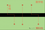
In my experience, the term “ground loop” can refer to any situation in which a system is affected by a difference in ground potential. A typical example is when two modules are connected by a long cable and the return current in the cable causes one module’s ground voltage to be significantly higher than the other module’s ground voltage. In this discussion, though, I’m referring specifically to a loop of ground connections; for example:
-- 術(shù)語“地面回路”可以指系統(tǒng)受“地電位差”影響的任何情況。 一個(gè)典型的例子是當(dāng)兩個(gè)模塊通過長(zhǎng)電纜連接時(shí),電纜中的返回電流導(dǎo)致一個(gè)模塊的接地電壓明顯地高于另一個(gè)模塊的接地電壓。 在這里,作者指的是一個(gè)接地環(huán)路, 例如下圖:
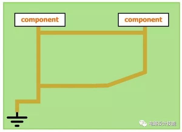
If you have to make numerous ground connections using individual PCB traces, it would not be difficult to create a loop like the one shown above. If you’ve readmy article on mutual inductance, you know that this sort of conductive loop is a good receiver of magnetic interference.
--如果必須使用單獨(dú)的PCB走線進(jìn)行多個(gè)地方的接地連接,會(huì)很容易出現(xiàn)上面的環(huán)路,這種導(dǎo)電環(huán)路非常容易接收磁干擾(像天線一樣,有時(shí)候示波器探頭的接地線也會(huì)形成受干擾的環(huán)路)。
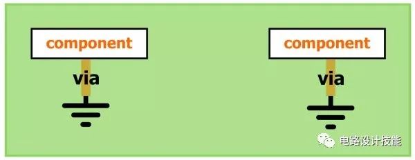
The presence of a ground plane does not make it impossible to create a ground loop, since the CAD program won’t prevent you from drawing traces between ground points. But if you consistently make your ground connections using vias or through-holes, the problem should largely disappear: by dropping vias to the plane you are making a direct connection from the component to a ground point that is connected through low impedance to all other ground points in the circuit.
-- 使用了地平面并不意味著你不會(huì)產(chǎn)生這種接地回路,PCB的設(shè)計(jì)工具無法阻止你在各個(gè)接地點(diǎn)之間進(jìn)行連線。如果你習(xí)慣了使用過孔或通孔進(jìn)行接地連接,上面的問題就很容易避免:通過過孔直接連接“地平面”,元器件到任何一點(diǎn)“地”之間的連接阻抗都非常低。
An Integrated Shield
A solid ground plane provides some degree of protection againstelectromagnetic interference(both radiated and received). I wouldn’t rely on a ground plane to solve all of your EMI problems, especially if you have components on both sides of the board; a carefully designed conductive enclosure would be more effective. Nonetheless, every little bit helps, and if you’re concerned about EMI then you have one more reason to incorporate a ground plane into your layout.
-- 接地平面還能夠防止電磁干擾(輻射和接收)。當(dāng)然不要指望接地平面來解決所有的EMI問題,尤其是電路板的兩側(cè)都有元件的時(shí)候,用導(dǎo)電外殼會(huì)更有效。盡管如此,接地平面的使用對(duì)于EMI的改善還是有一定幫助的。
The PCB-Plane Capacitor
This is not a major benefit, and it applies only to ground planes that are adjacent to a power plane. I think it’s still worth mentioning, though. A ground plane separated from a power plane by a thin dielectric sounds a lot like a parallel-plate capacitor, and that’s exactly what it is. This structure adds a bit of distributed power-supply capacitance to your entire circuit board, though it certainly isn’t going to replace yourdecoupling capacitors.
-- 與電源平面相鄰的地平面會(huì)形成“板間電容”,為整個(gè)電路板增加了一些分布式電源電容,起到一定的去耦作用,雖然無法完全取代你電路中的去耦電容。
Practical Impediments
I cannot imagine a scenario in which a four-layer PCB would not have a ground plane. I suppose it’s possible that a very dense layout would need both internal layers for normal signal routing, but honestly that seems unlikely: there’s no doubt that the plane occupies routing area, but by simplifying ground connections it also reduces the amount of routing area that the board will require.
-- 四層PCB板一般都要有地平面,當(dāng)然有兩個(gè)平面(電源平面和地平面)會(huì)更好,多用“平面”會(huì)減少信號(hào)走線層,但因?yàn)橛辛恕捌矫妗睍?huì)簡(jiǎn)化布線的難度。用多少個(gè)平面要根據(jù)實(shí)際的情況綜合考慮作出平衡。
A much more realistic scenario is that a ground plane is omitted because schedule or budgetary concerns argue in favor of a two-layer board. Now the ground plane is consuming one of only two PCB layers. Is it really better to include a ground plane if that means cramming almost all of the traces and components onto one layer? In my opinion, yes, it’s still better to include a ground plane, unless the circuit is so straightforward that you can use well-organized, low-impedance traces to make your ground connections. But honestly, if your space constraints are so extreme that you can’t make the board large enough to accommodate a ground layer on the bottom and a clean layout on the top, you should move to a four-layer board.
-- 兩層板的設(shè)計(jì)中是否應(yīng)該拿出一層來做地平面呢?這將意味著幾乎所有的走線和器件都要在一層上搞定,作者認(rèn)為,這是值得的,有地平面會(huì)更好,可以使用組織良好的低阻抗走線來建立接地連接。如果板子的空間限制非常嚴(yán)重,以至于無法使電路板足夠大以容納底部的接地層和頂部的干凈布局走線,就應(yīng)該考慮用4層板。
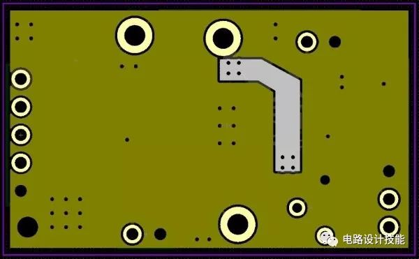
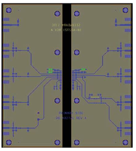
這是作者曾經(jīng)設(shè)計(jì)的2層電路板的接地層,接地平面不必100%都是“地”,必要的時(shí)候也可以拿出一部分用于必須的走線。
Summary
Adding a ground plane to your PCB is a simple, low-cost, highly effective way to design electronic devices that have better signal integrity, higher accuracy, and more resistance to interference. If you’re not in the habit of incorporating a ground plane, make sure to keep these benefits in mind when it comes time to lay out your next board.
-- 在PCB上添加接地平面是一種簡(jiǎn)單、低成本、高效的方法來設(shè)計(jì)具有更好信號(hào)完整性、更高精度和更強(qiáng)抗干擾性的電子產(chǎn)品。因此在設(shè)計(jì)PCB的時(shí)候應(yīng)盡可能養(yǎng)成使用接地平面的習(xí)慣。
-
電路
+關(guān)注
關(guān)注
173文章
6022瀏覽量
174561 -
pcb
+關(guān)注
關(guān)注
4357文章
23438瀏覽量
407166
原文標(biāo)題:PCB設(shè)計(jì)中為什么盡量用地平面?
文章出處:【微信號(hào):xiaojiaoyafpga,微信公眾號(hào):電子森林】歡迎添加關(guān)注!文章轉(zhuǎn)載請(qǐng)注明出處。
發(fā)布評(píng)論請(qǐng)先 登錄
電路PCB的地平面設(shè)計(jì)對(duì)EMI的影響
電源/地平面對(duì)的模型
接地平面(轉(zhuǎn)載)(不針對(duì)PCB板天線)
PCB布局提示和技巧:盡可能使用地平面
混合信號(hào)PCB設(shè)計(jì)中地平面鋪設(shè)方式和單點(diǎn)接地
【高速PCB布線指南3】接地平面漫談
內(nèi)層的電源平面、地平面如何設(shè)計(jì)?
降低PCB的KMI無疑是成功的PCB設(shè)計(jì)!
PCB軟件性能怎樣影響電源平面和地平面的布局?
淺談PCB設(shè)計(jì)產(chǎn)生EMI的問題
電源地平面的分割技巧

PCB地平面分割設(shè)計(jì)
淺談完整地平面的重要性


 工商網(wǎng)監(jiān)
評(píng)論